1. Introduction to binary multiplication
The binary number multiplication process can be modeled as the decimal number multiplication. But since binary numbers have only two possible multiplier bits, 0 or 1, binary multiplication is simpler. The rule of binary number multiplication is: 0X0=0,01=1X0=0,1X1=1.

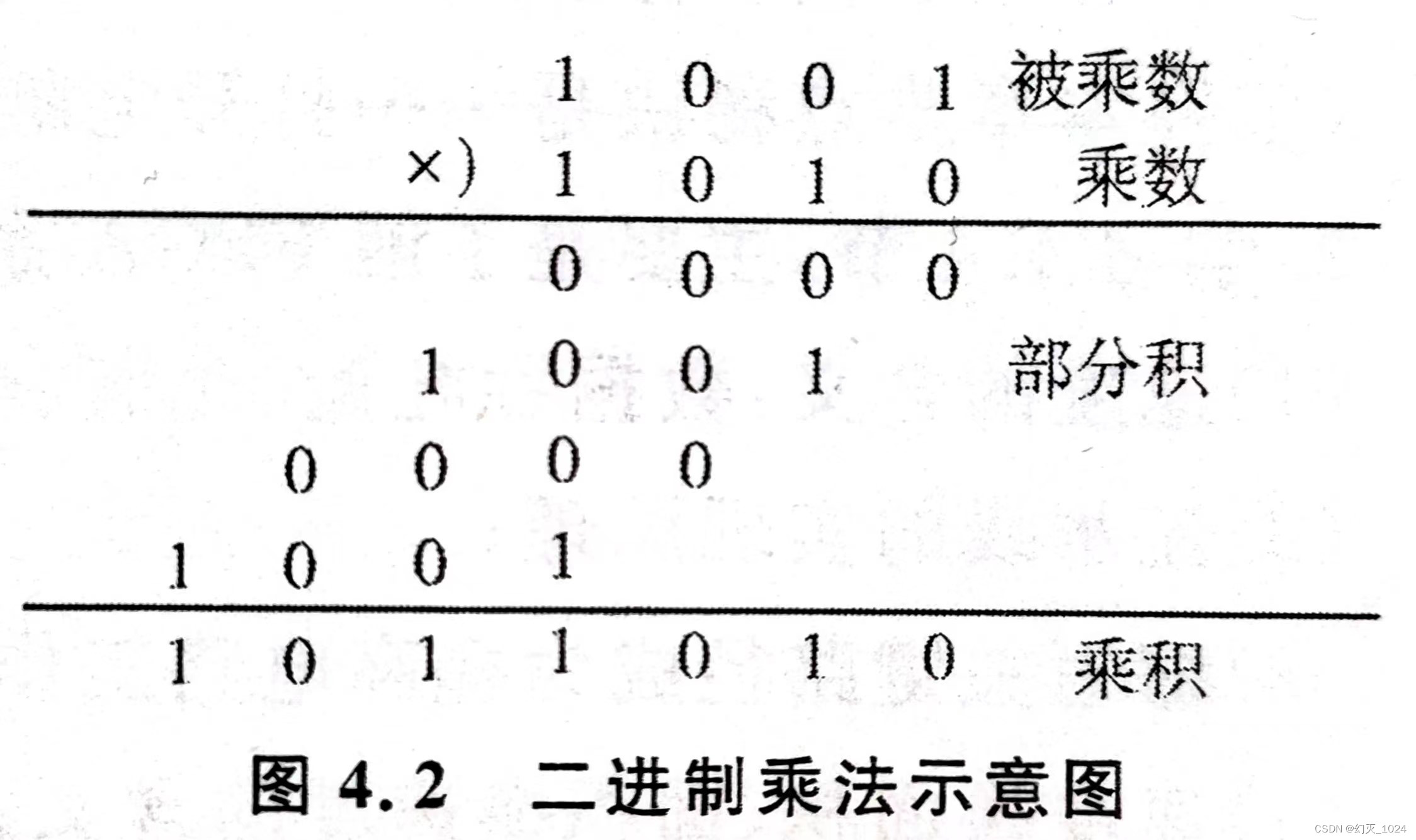
From the low bit to the high bit, use each bit of the multiplier to multiply the multiplicand. If a bit of the multiplier is 1, the sub-part product is the multiplicand; if a bit of the multiplier is 0, the multiplicand The subpart product is 0. The lowest bit of a certain partial product must be aligned with the standard multiplier, and the result of adding all partial products is the product obtained by multiplication.
2. Flow chart design:
According to the above algorithm, first design a flow chart of binary multiplication, as shown in Figure 4. The first step in the flow chart is the idle step. In this step, the circuit does not do any work, waiting for the input of the multiplier and multiplicand and START signal input. After detecting that the START signal is valid, the circuit enters the initialization state, and in this state, the P product term, the G carry terminal and the C counter are cleared.
Then the circuit judges whether Qlsb, that is, the least significant bit of the Q register is 1. If it is 1, the addition operation of the high 4 bits of P and the R register is completed, and the carry bit is G. If Qlsb is 0, skip the addition operation and directly enter the shift operation. After the addition of P and R, the next step is to directly jump to the shift operation. In the shift step, the right shift operation of P and Q is completed, and the operation of adding 1 to the C counter is completed at the same time.
After the shift step, it is judged whether C is equal to 3. If it is equal to 3, it will directly enter the done step, and the multiplication calculation process ends. Otherwise, go to the step of judging Q_lsb again. The next step is to complete 4 shift operations in the flow chart as described above. Therefore, the final result of C should be 4. The judgment here is whether it is equal to 3 or not, considering that the circuit is in the process of implementation The result of adding 1 will only appear in the next cycle. In the current clock cycle, it can only be judged whether the result is equal to 4 or not.
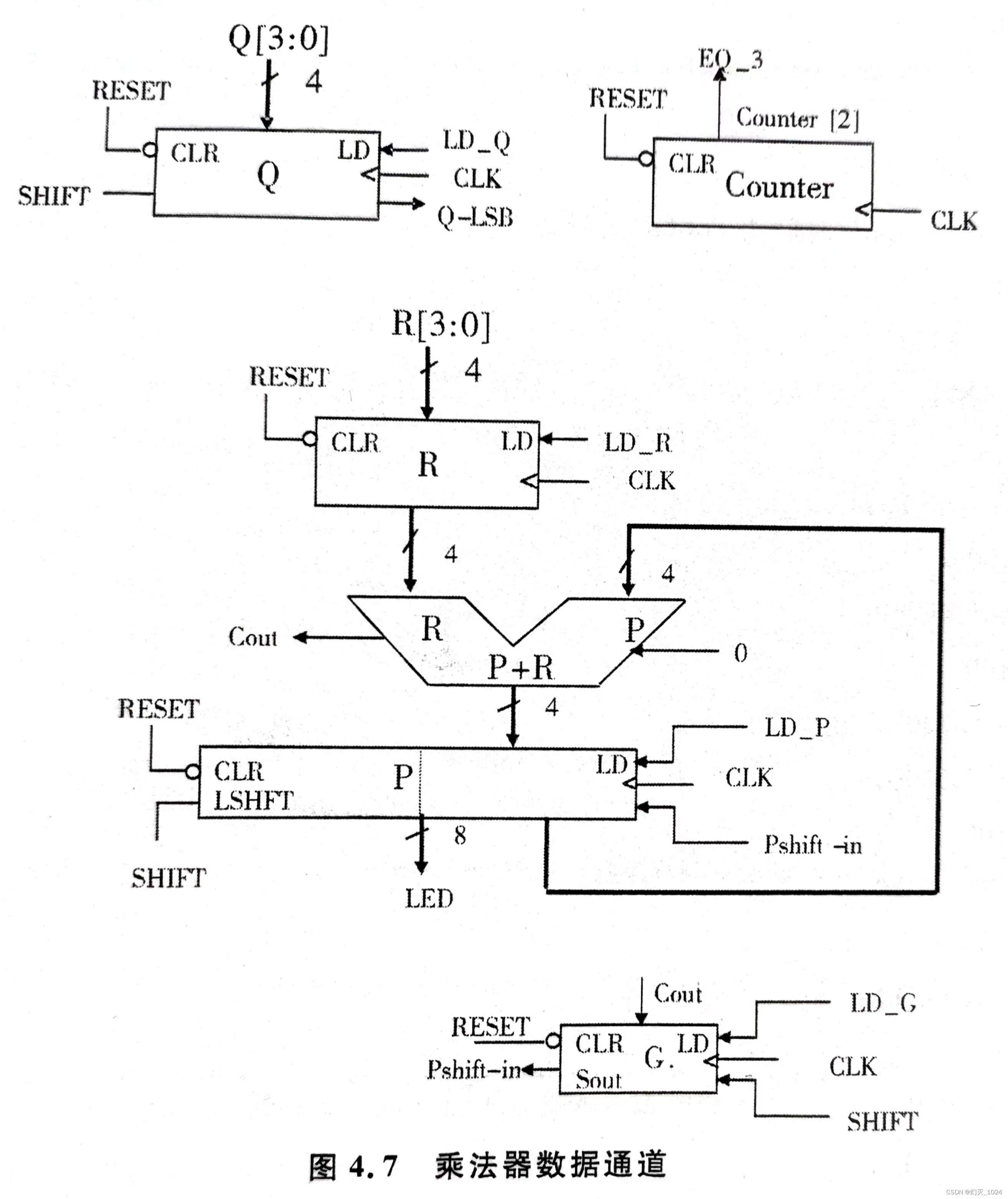
3. Data channel design:
The data channel comes from the interpretation of the flow chart, and the flow chart is decomposed below. It can be seen in the flowchart that the R register is required to store the multiplicand. The Q shift register is needed, which can perform right shift operation and save data; the product term register P is needed in the circuit, and P can realize the right shift function and the data save function.
The G carry register is required, and this register can also realize the right shift function. An adder is needed during the addition operation. The adder completes the addition of the high 4 bits of P and the R multiplicand. The result of the addition is stored in the P register, and the carry bit is stored in the G register. A counter is needed in the counting process, and the counter counts once every time it completes a shift operation. The specific data channel is shown in Figure 4.7.
//DataPath overall data channel
module datapath(
    clk, clr, shift, cnt_en, ld_P, ld_R,
    ld_Q, ld_g, R, Q, P, eq_3, Q_lsb,
    P_H_OUT, P_L_OUT, ge, shi, bai, R_shi, Q_shi, R_ge, Q_ge
    );
input clk, clr, shift, cnt_en, ld_P, ld_R, ld_Q, ld_g;
input [3:0] R,Q;
output [7:0] P;
output [3:0] P_H_OUT,P_L_OUT,ge,shi,bai,R_shi,Q_shi,R_ge,Q_ge;
output eq_3;
output Q_lsb;
wire [3:0]R_to_add;//R register output
wire [3:0]R_and_P;//The sum of R and P
wire cout;//adder carry output
wire G_to_P;//G register output
wire [3:0]P_H_OUT;//P register high output
wire P_H_lsb;//The lowest bit of the high bit of the P register
wire [3:0] CQ,CR;
// instantiate comparator module
comparator comp(.a(R),.b(Q),.CR(CR),.CQ(CQ));

//Instantiate the shift register
shift_reg Qreg(
.clk(clk),
.reset(clr),
.shift(shift),
.load(ld_Q),
.in_data(CQ),
.shift_in_data(1'b0),
.shift_reg(),
.shift_reg_lsb(Q_lsb)
);
//Instantiate the shift register
shift_reg Rreg(
.clk(clk),
.reset(clr),
.shift(1'b0),
.load(ld_R),
.in_data(CR),
.shift_in_data(1'b0),
.shift_reg(R_to_add),
.shift_reg_lsb()
);

//Instantiate the shift register
shift_reg P_Hreg(
.clk(clk),
.reset(clr),
.shift(shift),
.load(ld_P),
.in_data(R_and_P),
.shift_in_data(G_to_P),
.shift_reg(P_H_OUT),
.shift_reg_lsb(P_H_lsb)
);

//Instantiate the shift register
shift_reg P_L(
.clk(clk),
.reset(clr),
.shift(shift),
.load(1'b0),
.in_data(4'b0),
.shift_in_data(P_H_lsb),
.shift_reg(P_L_OUT),
.shift_reg_lsb()
);
//Instantiate the C counter
counter counter(
.clk(clk),
.clr(clr),
.cnt_en(cnt_en),
.eq_3 (eq_3)
);
//instantiate adder
adder adder(
.a(R_to_add),
.b(P_H_OUT),
.c(cout),
.sum(R_and_P)
);
//Instantiate the G register
G_reg G_reg(
    .clk(clk),
    .ld_g(ld_g),
    .din(cout),
    .dout(G_to_P),
    .clr (clr)
);
assign P = {P_H_OUT,P_L_OUT};
//Instantiate a hundred conversion modules
Multiplier_out Multiplier_out(
    .sumin(P),
    .ge(ge),
    .shi(shi),
    .bai(bai)
);
//Instantiate a hundred conversion modules
Multiplier_out R_out(
    .sumin(R),
    .ge(R_ge),
    .shi(R_shi),
    .bai()
);
//Instantiate a hundred conversion modules
Multiplier_out Q_out(
    .sumin(Q),
    .ge(Q_ge),
    .shi(Q_shi),
    .bai()
);

endmodule
4. State machine design:
The state machine is shown in the figure, and the state machine is drawn according to the flow chart. Each action in the flow chart corresponds to a state, so 5 states are required. The following describes each state separately. Idle is an idle state. No matter what state the circuit is in, when the reset signal is valid, the circuit must enter the idle state. In the idle state, the next state enters the init state when the start signal is valid, otherwise the next state is still waiting in the idle state. In the init state, if the input signal Q_Isb is 1, the next state will enter the add state, otherwise the next state will enter the shift state. The down-state of the add state goes directly to the shift state. In the shift state, if the egl_3 signal is 1, the next state enters the done state, otherwise check whether the Q_lsb signal is valid, if the eql_3 signal is 0 and the Q_lsh signal is 1, the next state of the shift state enters the add state state. If the eql_3 signal is 0 and the Q_lsb signal is 0, the next state of the shift state enters the shift state. The next state of the done state is still done, and returns to the idle state until the circuit reset signal is valid.


//state machine
module state_machine(clk, reset, clr, shift, ld_P, ld_R, ld_Q, ld_g, eq_3, Q_lsb, START, DONE, cnt_en, present_state, next_state);
input clk,reset,eq_3,START,Q_lsb;
output shift, ld_P, ld_R, ld_Q, ld_g, DONE, clr, cnt_en, present_state, next_state;
reg shift, ld_P, ld_R, ld_Q, ld_g, DONE, clr, cnt_en;
reg [2:0]c;//present_state is the current state, next_state is the next state
reg [2:0] present_state, next_state;
parameter idle=3'b000;//idle state
parameter init=3'b001;//initialization status
parameter add=3'b010;//addition status
parameter Shift=3'b011;//Shift state
parameter done=3'b100;//completion status
parameter empty=3'b101;//delay status
always@(posedge clk,negedge reset)
if(1'b0==reset)//When reset is low level, the state machine returns to the idle state
    present_state<=idle;
else
    present_state<=next_state;//Otherwise the state machine enters the next state
always@(present_state,eq_3,START,Q_lsb)
case(present_state)
idle:begin if(1'b0==START)//When START is pressed
    next_state=init;
    else
    next_state=idle;//Otherwise the state machine is still in idle state
    {shift, ld_P, ld_Q, ld_R, ld_g, cnt_en, DONE, clr}=8'b00000000;//The output of the state machine
end
init:begin if(1'b1==Q_lsb)//When Q_lsb is high level, the state machine enters the addition state
    next_state=add;
    else
    next_state=empty;//Otherwise the state machine is still in the initialization state
    {shift, ld_P, ld_Q, ld_R, ld_g, cnt_en, DONE, clr}=8'b00110001;//The output of the state machine
end
add:begin
    next_state=empty;//The state machine enters the shift state
    {shift, ld_P, ld_Q, ld_R, ld_g, cnt_en, DONE, clr}=8'b01001001;//The output of the state machine
    end
Shift:begin
    if(1'b1==eq_3)//When eq_3 is high, the state machine enters the completion state
        next_state=done;
        else
        if(!eq_3 & amp; & amp; Q_lsb)
            next_state=add;//Otherwise the state machine is still in the shift state
            else
            next_state=Shift;//Otherwise the state machine is still in the shift state
            {shift, ld_P, ld_Q, ld_R, ld_g, cnt_en, DONE, clr}=8'b10001101;//Initialize the output of the state machine
    end
empty:begin
    {shift, ld_P, ld_Q, ld_R, ld_g, cnt_en, DONE, clr}=8'b00000001;//The output of the state machine
    next_state=Shift;//Otherwise the state machine enters the completion state*/
end
done:begin
/*
    next_state<=done;//The state machine enters the delay state
    {shift, ld_P, ld_Q, ld_R, ld_g, cnt_en, DONE, clr}=8'b00000011;//The output of the state machine
*/
{shift, ld_P, ld_Q, ld_R, ld_g, cnt_en, DONE, clr}=8'b00000011;//The output of the state machine
\t
if(1'b0==START)begin//When START is pressed
     next_state=idle;
//{shift,ld_P,ld_Q,ld_R,ld_g,cnt_en,DONE,clr}=8'b00000000;//The output of the state machine
end
    else begin
    next_state=done;//Keep the current state
    end

end
  default: next_state=idle;
end case
endmodule
5. Top-level design:
//top-level design
module Multiplier(
    START, done, clk, reset, Q,
    R, P, present_state, next_state,
    eq_3, Q_lsb, P_H_OUT,
    P_L_OUT,shift,ge,shi,bai,
    data_ge, data_shi, data_bai,
R_shi, Q_shi, R_ge, Q_ge,
data_Q_shi, data_R_ge, data_R_shi, data_Q_ge
    );
input START,clk,reset;
input [3:0] R,Q;
output [7:0] P;
output [3:0] P_H_OUT,P_L_OUT,ge,shi,bai,R_shi,Q_shi,R_ge,Q_ge;
output [2:0] present_state, next_state;
output done, eq_3, Q_lsb, shift;
wire done;
wire shift, ld_P, ld_R, ld_Q, ld_g, clr, cnt_en, eq_3, Q_lsb;
wire [7:0] P;
wire [3:0] P_H_OUT,P_L_OUT;
output [6:0] data_ge, data_shi, data_bai, data_Q_ge, data_Q_shi, data_R_ge, data_R_shi;
wire [6:0] data_ge, data_shi, data_bai, data_Q_ge, data_Q_shi, data_R_ge, data_R_shi;
//Instantiate the state machine
state_machine state_machine(.clk(clk),.reset(reset),.cnt_en(cnt_en),
.clr(clr), .shift(shift), .ld_P(ld_P), .ld_R(ld_R), .ld_Q(ld_Q), .ld_g(ld_g),
.eq_3(eq_3),.Q_lsb(Q_lsb),.START(START),.DONE(done),
.present_state(present_state), .next_state(next_state));
//Instantiate the data path
datapath datapath(
.clk(clk), .clr(clr), .shift(shift),
.cnt_en (cnt_en), .ld_P (ld_P), .ld_R (ld_R),
.ld_Q(ld_Q), .ld_g(ld_g), .R(R), .Q(Q),
.P(P), .eq_3(eq_3), .Q_lsb(Q_lsb),
.P_H_OUT(P_H_OUT), .P_L_OUT(P_L_OUT),
.ge(ge), .shi(shi), .bai(bai), .R_ge(R_ge),
.R_shi(R_shi),.Q_ge(Q_ge),.Q_shi(Q_shi)
);
//Instantiate the digital tube module
 seven_seg out_ge(
   .num1(ge),
   .data1(data_ge)
);
//Instantiate the digital tube module
 seven_seg out_shi(
   .num1(shi),
   .data1(data_shi)
);
//Instantiate the digital tube module
 seven_seg out_bai(
   .num1(bai),
   .data1(data_bai)
);
//Instantiate the digital tube module
 seven_seg out_R_ge(
   .num1(R_ge),
   .data1(data_R_ge)
);
//Instantiate the digital tube module
 seven_seg out_R_shi(
   .num1(R_shi),
   .data1(data_R_shi)
);
//Instantiate the digital tube module
 seven_seg out_Q_ge(
   .num1(Q_ge),
   .data1(data_Q_ge)
);
//Instantiate the digital tube module
 seven_seg out_Q_shi(
   .num1(Q_shi),
   .data1(data_Q_shi)
);
endmodule
6. Shift register module
//shift register (general purpose)
module shift_reg(clk,reset,in_data,shift,load,shift_reg_lsb,shift_in_data,shift_reg);
input clk,reset,shift,load;
input [3:0] in_data;
input shift_in_data;
output shift_reg_lsb;
output [3:0] shift_reg;
reg [3:0] shift_reg;
always @(posedge clk,negedge reset)
    if(1'b0===reset)//reset is low, the register is cleared
        shift_reg<=4'b0;
    else if(1'b1===load)//When load is high level, assign in_data to shift_reg
        shift_reg<=in_data;
    else if(1'b1===shift)//shift is high, shift shift_reg left one bit
        shift_reg<={shift_in_data,shift_reg[3:1]};
    else
        shift_reg<=shift_reg;//otherwise shift_reg remains unchanged
assign shift_reg_lsb=shift_reg[0];//shift_reg_lsb is the lowest bit of shift_reg
endmodule

//C counter
module counter(clk,clr,cnt_en,eq_3);
input clk, clr, cnt_en;
output eq_3;
reg eq_3;
reg [2:0] cnt_reg;
always@(posedge clk,negedge clr)
if(1'b0==clr)//clr is low, the counter is cleared
    cnt_reg<=3'b0;
else if(1'b1==cnt_en)//When cnt_en is high level, the counter is incremented by one
    cnt_reg<=cnt_reg + 1'b1;
    else
    cnt_reg<=cnt_reg;//Otherwise the counter remains unchanged
always@(cnt_reg)
if(3'b100==cnt_reg)//When the counter is 3, eq_3 is high
    eq_3=1'b1;
else
    eq_3=1'b0;//otherwise eq_3 is low level
endmodule
7. Adder module
//adder
module adder(a,b,c,sum);
input [3:0] a,b;
output [3:0] sum;
output c;
reg [3:0] sum;
reg c;
always@(a,b)
{c,sum}=a + b;
endmodule
8.G register module
//G register
module G_reg(clk,ld_g,din,dout,clr);
input clk, ld_g, din, clr;
output dout;
reg dout;
always@(posedge clk)
if(clr==1'b0)//When clr is low level, the G register is cleared
    dout<=1'b0;
else if(ld_g)//When ld_g is high level, assign din to dout
    dout<=din;
else
    dout<=dout;//Otherwise dout remains unchanged
endmodule
9. Other modules
//Seven-segment digital tube module
module seven_seg(num1,data1);
input[3:0]num1;
output [6:0]data1;
reg[6:0]data1;
always@(num1) begin
case (num1)
      4'd0: begin data1 = 7'b1000000; end
4'd1: begin data1 = 7'b1111001; end
4'd2: begin data1= 7'b0100100; end
4'd3: begin data1 = 7'b0110000; end
4'd4: begin data1 = 7'b0011001; end
4'd5: begin data1 = 7'b0010010; end
4'd6: begin data1 = 7'b0000010; end
4'd7: begin data1 = 7'b1111000; end
4'd8: begin data1 = 7'b0000000; end
4'd9: begin data1 = 7'b0010000; end
      default: begin data1 = 7'b0000001; end
end case
end
endmodule

//digital conversion module
module Multiplier_out(
    sumin, // multiplier output
    ge,//unit
    shi,//ten
    bai,//hundreds
);
input [7:0]sumin;
output [3:0]ge,shi,bai;
reg [3:0]ge,shi,bai;
always@(sumin) begin
    bai=sumin/100;//hundreds
    shi=(sumin-bai*100)/10;//ten digits
    ge=sumin-bai*100-shi*10;//unit
end
endmodule

// compare converter module
module comparator(
    a,b,//comparison number
    CQ, CR
);
input [3:0]a,b;
output [3:0]CQ,CR;
reg [3:0]CQ,CR,TMP;
always@(a,b) begin
    if(a>b) begin
CR<=b;
CQ<=a;
end
    else
begin
        CR<=a;
        CQ<=b;
end
end
endmodule