1. Foreword
In the past two years, the requirements and difficulty of graduation projects and graduation defenses have continued to increase. Traditional graduation projects lack innovation and highlights, and often fail to meet the requirements for graduation defenses. In the past two years, junior students and junior students have constantly told Senior Xiaohong to do it himself The project system does not meet the teacher’s requirements. In order for everyone to pass the graduation project smoothly and with the least amount of energy, Senior Xiao Hong shared a high-quality graduation project. Today I want to share a temperature and humidity control servo switch based on the 51 microcontroller Bluetooth upload.
2. Introduction
Based on 51 microcontroller Bluetooth upload temperature and humidity control servo switch
1. You can select sending and receiving modes, manual and automatic modes through the hexagonal switch.
2. In the sending mode, the temperature and humidity are automatically reported. In the receiving mode, it is divided into automatic mode. If the light intensity exceeds the set threshold or the raindrop sensor detects raindrops, the servo will turn to 90 degrees.
3. If the light intensity does not exceed the set threshold or the raindrop sensor does not detect raindrops, the servo will turn to 90 degrees.
4. In manual mode, you can send the command “*” through the Bluetooth of the mobile phone APP, and the servo will turn back to 0 degrees; the mobile phone will send the command “#” through Bluetooth, and the servo will turn to 90 degrees.
6. In manual mode, the light sensor and raindrop sensor are disabled.
7. Both the raindrop sensor and the light sensor can adjust the detection sensitivity through the potentiometer on the sensor.
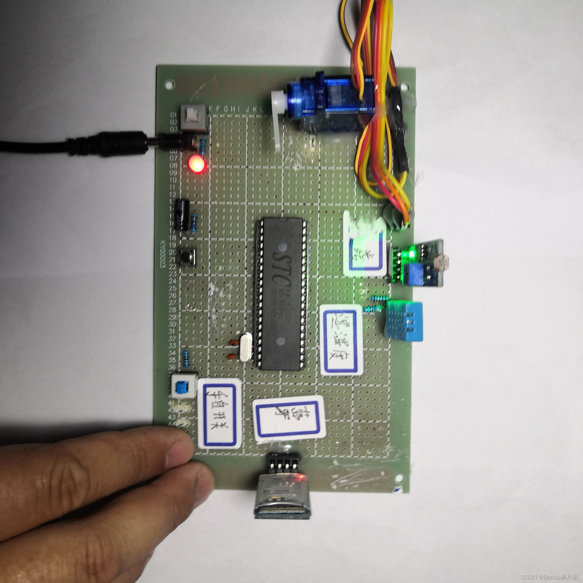
3. Composition
This system consists of STC89C52 microcontroller circuit + raindrop sensor circuit + light sensor + temperature and humidity sensor + Bluetooth module circuit + steering gear circuit (simulated awning) + switch circuit + power circuit
4. Realize the effect
Overall display
5. Design principle
5.1 Introduction to STC89C52RC
The STC89C52RC microcontroller has a wide range of uses and is the first choice chip for every electronic equipment designer. This chip is deeply loved by the majority of users. This microcontroller is enhanced and modified based on the 8051 microcontroller. It is fully compatible with the traditional 8051 microcontroller when writing instruction codes, so it is more convenient to write programs. Its advantages are high reliability, affordable price and low power consumption. The main technical advantage of the STC89C52RC microcontroller chip is the use of Flash memory technology. The use of this technology not only reduces the manufacturing cost, but also It is fully compatible with the 8051 microcontroller in terms of software and hardware. It is also manufactured using high-density non-volatile memory manufacturing technology and combines a multi-functional 8-bit CPU and flash memory in a single chip, so it can be accepted by most users in China. . The electrically rewritable nature of its program makes development and testing easier, and also provides a highly flexible and cheap solution for many embedded control systems.
There are 12 clocks/machine cycles and 6 clocks/machine cycles inside the chip, and we can choose at will. Its working voltage is: 5.5V ~ 3.3V (5V microcontroller) / 3.8V ~ 2.0V (3V microcontroller). Its working frequency is between 0 and 40MHz, which is more convenient than the ordinary 8051 microcontroller. In actual use, its working frequency can reach 48MHz. The application space we can use is 8K bytes, and 512 bytes of RAM are integrated on the chip. There are 32 general-purpose I/O ports on the chip, that is, 4 groups are P1, P2, P3, and P4. Each group has 8 I/O ports. The four groups of interfaces after reset are quasi-bidirectional ports/weak pull-ups. When used as bus expansion, there is no need to add a pull-up resistor, but when used as an I/O port, a pull-up resistor is required. The built-in ISP (In-System Programmable) and IAP (In-Application Programmable) technologies within the chip make programming and simulation very easy, eliminating the trouble of using a dedicated programmer and a dedicated emulator, and can also be used directly Download the user program through the serial port (RxD/P3.0, TxD/P3.1), the download speed is very fast, which makes the programming of the program easier. There is also a watchdog function. 4 external interrupts, falling edge interrupt or low level trigger circuit, Power Down mode can be woken up by external interrupt low level trigger interrupt. There are three 16-bit timers/counters, namely timers T0, T1, and T2. Universal asynchronous serial port (UART), timer software can also be used to implement multiple UARTs.
STC89C52RC pin function description:
VCC (40 pin): supply voltage
VSS (20 pin): ground
P0 port (P0.0~P0.7, pins 39~32): Port P0 is an open-drain 8-bit bidirectional I/O port. As an output port, each pin can drive 8 TTL loads. When “1” is written to port P0, it can be used as a high-impedance input. When accessing external program and data memory, Port P0 can also provide a multiplex bus for the lower 8-bit address and 8-bit data. At this time, the internal pull-up resistor of port P0 is effective. When programming Flash ROM, the P0 port receives the instruction byte; when verifying the program, the instruction byte is output. During verification, an external pull-up resistor is required.
P1 port (P1.0~P1.7, pins 1~8): Port P1 is an 8-bit bidirectional I/O port with internal pull-up resistor. The output buffer of P1 can drive (sink or source current mode) 4 TTL inputs. When writing 1 to the port, the port is pulled to a high potential through the internal pull-up resistor, which can be used as an input port. When port P1 is used as an input port, because of the internal pull-up resistor, those pins that are externally pulled low will output a current.
P2 port (P2.0~P2.7, 21~28 pins): P2 port is an 8-bit bidirectional I/O port with internal pull-up resistor. The output buffer of P2 can drive (sink or source current mode) 4 TTL inputs. When writing 1 to the port, the port is pulled to a high level through the internal pull-up resistor, and then it can be used as an input port. When P2 is used as an input port, because of the internal pull-up resistor, those pins that are pulled low by external signals will output a current.
When accessing external program memory and external data memory with a 16-bit address (such as executing the “MOVX @DPTR” instruction), P2 sends the high 8-bit address. When accessing an external data memory with an 8-bit address (such as executing the “MOVX @R1” instruction), the contents of the P2 port pin (that is, the contents of the P2 register in the special purpose register (SFR) area) will not be used during the entire access. Change. During Flash ROM programming and program verification, P2 also receives high-order addresses and some control signals.
P3 port (P3.0~P3.7, pins 10~17): P3 is an 8-bit bidirectional I/O port with internal pull-up resistor. The P3’s output buffer can drive (sink or source current mode) 4 TTL inputs. When writing 1 to the port, the port is pulled to a high potential through the internal pull-up resistor, and it can be used as an input port. When P3 is used as an input port, because of the internal pull-up resistor, those pins that are pulled low by external signals will input a current.
The chip pin diagram of the STC89C52RC microcontroller is as shown in the figure.

Figure STC89C52RC microcontroller pin diagram
Crystal oscillator circuit
There is a crystal oscillator circuit in every single-chip microcomputer system, and the crystal oscillator plays a decisive role in the entire single-chip microcomputer system. It combines the internal circuit of the microcontroller to generate a clock frequency. With this basic microcontroller, the microcontroller can execute all instructions and complete the required functions. At the same time, the speed of the clock frequency directly affects the running speed of the microcontroller. The higher the clock frequency, the faster the corresponding microcontroller runs. Crystal oscillator is actually a crystal resonance technology that converts electrical energy and mechanical energy into each other, providing stable and accurate single-frequency oscillation for its microcontroller.
A crystal oscillator circuit generally consists of two capacitors, also called load capacitors. The working state of the microcontroller is generally in a parallel resonance state. The size of the load capacitance will be determined according to the requirements of the crystal oscillator. The frequency of the crystal oscillator is tested under the load capacitance it provides, so as to reduce the occurrence of errors. At the same time, it can also ensure the error caused by temperature drift. The same capacitor value is selected to ensure the normal operation of the crystal oscillator circuit. If the values of the two capacitors are different, or even the difference is too large, it will easily cause resonance imbalance and lead to shutdown. Vibrate or simply not vibrate.
In this design, XTAL1 and XTAL2 are externally connected to quartz crystals as timing components. There is a high-gain reverse amplifier inside the STC89C52RC chip to form an oscillator, thereby achieving self-oscillation and generating a clock. The operating frequency of the crystal oscillator is generally selected between 1.2~12MHZ, and the value of capacitors C1 and C2 is generally between 10PF~40PF. Here I chose an operating frequency of 12MHZ and two 22PF capacitors to form a crystal oscillator circuit. The crystal oscillator circuit of the STC89C52RC microcontroller is shown in Figure 3.2.

Figure crystal oscillator circuit
Reset circuit
The reset circuit is also an important part of the microcontroller. When the microcontroller starts running, it must first perform a reset operation. However, the microcontroller cannot complete it alone, so it must be combined with an external circuit to perform the reset operation. Figure 3.3 is the reset circuit diagram. The RST pin is the input for the reset signal. It is valid when the high level is input for more than two consecutive machine cycles. When the crystal oscillator frequency is 12MHZ, the reset signal should last for more than 2us to complete the reset operation. When we add a reset circuit and the microcontroller is powered on, the RST pin will first maintain a high level for a short period of time and then change to a low level. This is the process of resetting the microcontroller.

Figure reset circuit
6. Part of the core code

#include <reg52.h>
#include <intrins.h>
#include <stdio.h>
#include "dht21.h"

#define MODE_AUTO 0x01
#define MODE_OPTI 0x02

#define MODE_AUTO1 0x03
#define MODE_OPTI1 0x04

sbit key=P2^1; //Initial corresponding pin
sbit motor=P1^1; //Initial corresponding pin
sbit ligh=P1^0;
sbit relay=P1^2;
sbit setkey=P1^3;
sbit setkey1=P1^5;
sbit fengshan=P2^0;

unsigned int sum1=255;
unsigned int sum2=0;

bit motor_faly=0; //Read flag

unsigned int moTimHigh,moTimlow; //Motor control high and low level processing time

unsigned char setMode = MODE_AUTO; //Mode
unsigned char setMode1 = MODE_AUTO1; //Mode

unsigned long time_20ms=0; //Timing variable
unsigned char dis0[16]; //Array temporary storage
unsigned char read_dht21=0; //Read flag

void Init_Timer0(void);//Function declaration
void UART_Init(void);
void uartSendByte(unsigned char dat);
void SendStr(unsigned char *s,unsigned char length);

void main (void)
{
Init_Timer0(); //Timer 0 initialization
\t
UART_Init(); //Serial port initialization

DelayMs(120);
SendStr("ready ok!",9);