Southwest Jiaotong University Data and Electricity Experiment
Good place to practice writing HDL
Experiment requirements
1. Purpose of the experiment
1. Consolidate the design and simulation methods of combinational logic circuits.
2. Learn Verilog HDL hierarchical file design.
2. Experiment content
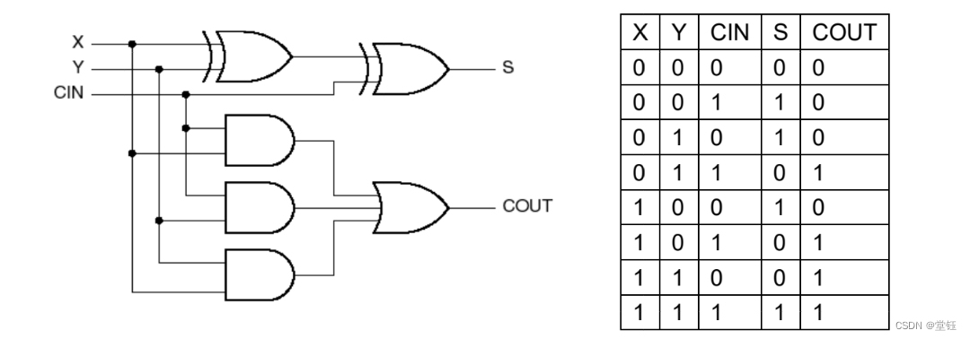
The experimental content follows the steps below to describe and simulate the illustrated circuit with Verilog HDL. This circuit implements 1-bit binary addition, X and Y are the addend and the summand respectively, CIN is the carry from the low bit, COUT is the carry to the high bit, and S is the sum of addition. The truth table is as follows:

edit
1. Gate-level description and simulation
(1) Create a new project file, the project name is: _student number_V1_1bit_adder_ga (1-bit adder gate-level description);
(2) Create a new Verilog HDL file and enter the code. Note: The name of the input and output ports must be exactly the same as the name on the picture, otherwise it cannot be simulated! [5 points]
(3) Select the menu Processing–Start Compilation, analyze and synthesize the circuit, if there is any error, please correct it yourself, screenshot the code and compile the report (Flow Summary); [5 points]
(4) Select the menu Tools-Netlist Viewers-RTL Viewer, and screenshot the logic circuit diagram; [5 points]
(5) Create the simulation vector waveform file Waveform.vwf, run the functional simulation (Simulation-Run Functional Simulation), take screenshots of the simulation results [5 points] and analyze whether the circuit function is correct [5 points].
Note: Each step requires screenshots, printing, and analysis
2. Data flow description and simulation. 【25 points】
Follow the steps in 1, create a new project named: _Student Number_V1_1bit_adder_df (1-bit adder data flow description), and complete the data flow modeling and simulation.
3. Behavioral modeling and simulation. 【25 points】
Follow the steps in 1, create a new project named: _Student Number_V1_1bit_adder_bh (1-bit adder behavior description), and complete the behavior modeling and simulation.
4. Structural modeling and simulation of 2-bit binary plus circuit. 【25 points】
Use the above adder (any one of the 3) to carry out structural modeling and simulation of the 2-bit binary adder (the simulation vector Waveform.vwf1 can be downloaded in the group file), the module name and port are defined as follows:
_Student number_V1_2bit_adder_st(a,b,ci,s,co); //2 is a binary addition structured modeling
input a[1:0], b[1:0]; //a is a 2-bit addend, b is a 2-bit addend
input ci; // carry input from low bit
output co; // carry output to the high bit
output s[1:0]; //The sum of 2 bits
Other requirements are the same as 1
5. Pin lock and download test
(1) Consult the pin number comparison table in the instruction manual of the experimenter, plan the pin locking, and fill in the pin locking table in the experiment report. Lock the input signal to the switch (main board device name SW0~SW15); lock the output signal to the indicator light (main board device name LED0~LED7).
(2) Start the Pin Planner of Quartus to complete the pin lock.
(3) Recompile the entire project. If there is an error, please correct it and recompile it.
(4) Connect the download cable to the experimenter and the computer correctly, and turn on the power of the experimenter.
(5) Start the Programmer, and download the generated sof file with the same name as the project to the core board of the experimenter in JTAG mode.
(6) Test and verify the 2-bit binary adder designed above on the experimental device.
(7) Record the measured results in the original record part of the experiment report in the form of a truth table.
3. Preview requirements
1. Find information by yourself, learn the hierarchical file design of Verilog HDL by yourself, and complete the design requirements of the “Experimental Content” part of this experiment.
2. Carry out functional simulation on the experimental circuit, and insert the screenshot of the simulation result into the report.
3. List the pin lock allocation table (signal name -> motherboard device name -> pin number).
4. Fill in the compilation report.
4. Experiment report requirements
1. List the power-on test results.
2. List the problems and solutions during the experiment.
3. Requirements for screenshots of code and comprehensive results
(1) There must be a file name (at the red line on the first line);
(2) The code and synthesis results must be complete.


4. Requirements for screenshots of simulation waveforms:
(1) There must be a file name (the first line);
(2) The signal name (name column on the left) must be clear and readable;
(3) The waveform must be clearly readable.
Example of a good simulated waveform

Bad waveform example

Verilog code and RTL circuit diagram
1. Gate-level description and simulation
a.Verilog code
module_1bit_adder_ga(X,Y,CIN,S,COUT);
input X,Y,CIN;
output S, COUT;
wire A1_xor;
wire A1_and, A2_and, A3_and;
xor
    n1(A1_xor,X,Y),
    n2(S,A1_xor,CIN);
and
    n3(A1_and,CIN,X),
    n4(A2_and,CIN,Y),
    n5(A3_and,X,Y);
or
    n6(COUT,A1_and,A2_and,A3_and);
endmodule
b. RTL circuit diagram

c. Simulation results

2. Data flow description and simulation
-
Verilog code
module_1bit_adder_df(X,Y,CIN,S,COUT);
input X,Y,CIN;
output S, COUT;
assign S = X^Y^CIN;
assign COUT = (CIN & amp; X) | (CIN & amp; Y) | (Y & amp; X);
endmodule
-
RTL circuit diagram

-
Simulation results

3. Behavioral modeling and simulation
a.Verilog code
module_1bit_adder_bh(X,Y,CIN,S,COUT);
input X,Y,CIN;
output S, COUT;
reg[2:0]A;
reg S,COUT;
always@(X,Y,CIN)
begin
    A[2] <=X;
    A[1] <=Y;
    A[0] <= CIN;
end
always@(A)
begin
    case(A)
        3'b000:S <= 0;
        3'b001:S <= 1;
        3'b010:S <= 1;
        3'b011:S <= 0;
        3'b100:S <= 1;
        3'b101:S <= 0;
        3'b110:S <= 0;
        3'b111:S <= 1;
    end case
    case(A)
        3'b000:COUT <= 0;
        3'b001:COUT <= 0;
        3'b010:COUT <= 0;
        3'b011:COUT <= 1;
        3'b100:COUT <= 0;
        3'b101:COUT <= 1;
        3'b110:COUT <= 1;
        3'b111:COUT <= 1;
    end case
end
endmodule
b. RTL circuit diagram

c. Simulation results

Four and 2-bit binary addition circuit structured modeling and simulation
a.Verilog code
module_1bit_adder_ga(X,Y,CIN,S,COUT);
input X,Y,CIN;
output S, COUT;
wire A1_xor;
wire A1_and, A2_and, A3_and;
xor
    n1(A1_xor,X,Y),
    n2(S,A1_xor,CIN);
and
    n3(A1_and,CIN,X),
    n4(A2_and,CIN,Y),
    n5(A3_and,X,Y);
or
    n6(COUT,A1_and,A2_and,A3_and);
endmodule

module_2bit_adder_st(a,b,ci,s,co);
input[1:0] a, b;
input ci;
output co;
output[1:0]s;
wire d;
_1bit_adder_ga(a[0],b[0],ci,s[0],d);
_1bit_adder_ga(a[1],b[1],d,s[1],co);
endmodule
b. RTL circuit diagram

c. Simulation results

The editor’s words
The content is for reference only.
After you understand it, it’s best to write it yourself. The first few experiments are quite simple. If you think about being lazy and don’t write it yourself, you may not know how to do the following experiments. You will also write it during the final exam. I can’t come out yet.
If you have any questions, please leave a message in the comment area!
Finally, thank you for your attention and support!