Directory
- 1. Create a project in CubeMX
- 2. Code writing to implement running lights
-
-
-
-
- 1. Write the code and implement it
- 2. Observe the output waveform of the GPIO port
-
-
-
- 3. Write code to control the turning on and off of the running water lamp by pressing the button
-
-
- 1. New construction
-
-
- (1) Configure interrupt function
- 2. Enter the NVIC interface to set the interrupt priority
- 3. Configure the clock
- 4. Generate project files
-
- 2. Write the code and implement it
-
1. Create a project in CubeMX
The java environment and CubeMX have been configured.
CubeMX official website download portal: CubeMX – Tools and Software
1.The first step

2. The second step

3.The third step

Set the “DEBUG” column in CubeMX to “Serial Wire”
It means you selected the Serial Wire Debug (SWD) interface as the debugging interface.
SWD is a debug interface protocol commonly used for debugging and programming interaction with ARM Cortex-M microcontrollers.
When you select the SWD interface, it will serve as the debug communication channel to the target chip. The SWD interface uses two wires for communication: SWDIO (Serial Wire Debug I/O) and SWCLK (Serial Wire Debug Clock). SWDIO is used for data transmission and debugging information sending and receiving, while SWCLK is used for clock synchronization.
By using the SWD interface for debugging, you can achieve the following functions:
- Single Step: Execute the code instruction by instruction to facilitate debugging the running process of the program.
- Breakpoint: Set a breakpoint at a specific line of code to stop program execution at the breakpoint for step-by-step debugging.
- Register viewing and modification: View and modify the register value of the target chip to analyze and debug the program status.
- Debug information output: Output debugging information to a development environment, such as a debugger or emulator, through the SWD interface.
In short, choosing to set the “DEBUG” column in CubeMX to “Serial Wire” means that you have selected the SWD interface as the debugging interface for debugging and developing embedded software.
4.The fourth step
In the STM32F103C8T6 microcontroller, the GPIO port is controlled and accessed through the APB2 bus.

In the STM32F103C8T6 microcontroller, HSE (High-Speed External) and LSE (Low-Speed External) are used to control different external clock sources respectively.
-
HSE(High-speed external clock):- Main clock (SYSCLK): HSE can be used as the main clock source to provide a higher clock frequency. With appropriate configuration and division coefficient, the frequency of HSE can be used as the system clock (SYSCLK).
- PLL (Phase Locked Loop) input: HSE can be used as the input clock source of the PLL for generating higher clock frequencies. By configuring the PLL parameters, the frequency of the HSE can be multiplied and output as SYSCLK.
-
LSE(low speed external clock):- RTC (Real Time Clock): LSE is used as the clock source for the RTC module of STM32F103C8T6. The RTC module is used to provide real-time clock and calendar functions, and can be used for timestamp recording, timer and alarm clock functions, etc.
Note: The STM32F103C8T6 microcontroller can also use internal clock sources (
HSIandLSI) as the main clock and RTC clock source.HSIis the internal high-speed clock, andLSIis the internal low-speed clock. Choosing to useHSEandLSEas the clock source is determined based on specific needs and application scenarios.
In the STM32F103C8T6 microcontroller, the clock of the APB2 bus is not directly controlled by the HSE (High Speed External Clock). The clock source of the APB2 bus can be selected from the system clock (SYSCLK) or the clock output from the PLL (Phase Locked Loop).
In STM32F103C8T6, HSE can be used as one of the input sources of the main clock (SYSCLK), and is output after being multiplied by the PLL. The main clock (SYSCLK) can be further divided to obtain the clock of the APB2 bus.
Specifically, the clock source configuration is as follows:
1. If HSE is configured as the input source of the main clock (SYSCLK), then the clock of the APB2 bus will also come from the output of HSE through the PLL.
2. If HSE is not configured as the input source of the main clock (SYSCLK), but uses an internal clock source (such as HSI), then the clock of the APB2 bus will be the same as the main clock (SYSCLK), from HSI or after multiplication by PLL Output HSI.
Therefore, the clock source of the APB2 bus is related to the main clock (SYSCLK) and is not directly controlled by HSE. Configuring the clock source of the main clock (SYSCLK) indirectly affects the clock frequency of the APB2 bus.
Therefore, in order to control the GPIO port through APB2, the choice here is to set HSE to Crystal/Ceramic Resonator.
5.The fifth step

Configure the corresponding pins as needed, click and select the pin mode. Select GPIO_Output here, output mode.

I added a button to A8 to do experiments on interrupt control. I chose GPIO_EXTI8
6.The sixth step
From the information provided above, if the HSE is configured as the input source of the main clock (SYSCLK), then the clock of the APB2 bus will also come from the output of the HSE through the PLL.

So select PLLCLK on the clock architecture page.
7. Step Seven
Generate code


2. Write code to implement running lights
1. Write code and implement
Because I rebuilt this project several times, for the sake of convenience, I changed the pins to this setting, leaving everything else unchanged.

Replace while(1){} in the main function with the following code.
 while (1)
  {<!-- -->
HAL_GPIO_WritePin(GPIOA,GPIO_PIN_4,GPIO_PIN_RESET);//PA4 lights up
HAL_GPIO_WritePin(GPIOB,GPIO_PIN_9,GPIO_PIN_SET);//PB9 lights out
HAL_GPIO_WritePin(GPIOC,GPIO_PIN_15,GPIO_PIN_SET);//PC15 lights out
HAL_Delay(1000);//Delay 1s
HAL_GPIO_WritePin(GPIOA,GPIO_PIN_4,GPIO_PIN_SET);//PA4 lights out
HAL_GPIO_WritePin(GPIOB,GPIO_PIN_9,GPIO_PIN_RESET);//PB9 lights up
HAL_GPIO_WritePin(GPIOC,GPIO_PIN_15,GPIO_PIN_SET);//PC15 lights out
HAL_Delay(1000);//Delay 1s
HAL_GPIO_WritePin(GPIOA,GPIO_PIN_4,GPIO_PIN_SET);//PA4 lights out
HAL_GPIO_WritePin(GPIOB,GPIO_PIN_9,GPIO_PIN_SET);//PB9 lights out
HAL_GPIO_WritePin(GPIOC,GPIO_PIN_15,GPIO_PIN_RESET);//PC15 lights up
HAL_Delay(1000);//Delay 1s
}
Explanation of the HAL_GPIO_WritePin(GPIOB,GPIO_PIN_9,GPIO_PIN_RESET); statement:
It is a HAL library function for GPIO output, which can set or change the current pin level value.
HAL_GPIO_WritePin(GPIO_TypeDef* GPIOX,Uint16_t GPIO_Pin,GPIO_PinState pinstate);
GPIOX represents the port number of the target pin, such as GPIOA
GPIO_Pin represents the pin number of the target pin
pinstate represents the high and low levels of the current pin, high level (GPIO_PIN_SET) and low level (GPIO_PIN_RESET).
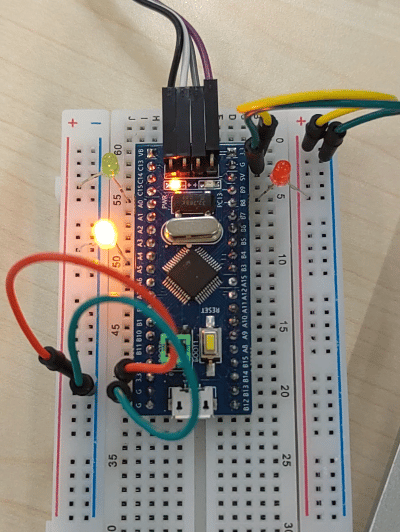
The running results are as follows
2. Observe the output waveform of the GPIO port
-
Click the magic wand in keil, enter the Target interface, and set the crystal oscillator to 8MHz

-
Enter the Debug interface and make the following settings, and finally click OK

-
Click Debug to enter debugging, open the logic analyzer (Logic Analyzer), and select the pin to be observed

-
Observe waveform

The dynamic image is as follows (there is a size limit for image uploading, so the speed is doubled):

It can be observed that the light with a low level on the pin is on, and the light with a high level is not on. The high-low level conversion period (LED flashing period) is about 1s.


3. Write code to control the turning on and off of the running light by pressing buttons
1. New construction
(1) Configure interrupt function

Setting the GPIO mode in CubeMX to “Rising and Falling Edge Triggered” means that you configure the input triggering mode of the GPIO pin so that it can be triggered at the pin level. Interrupts or events are triggered when rising and falling edges change.
When you set the GPIO mode to “Both rising and falling triggers”, the GPIO pin will monitor changes in its input level, and when the pin level changes from low level (0) to high level ( 1) or trigger the corresponding interrupt or event when changing from high level (1) to low level (0).
This triggering method is often used in application scenarios that require real-time response to changes in input signals. For example, when a button or switch is pressed or released, you can configure the corresponding GPIO pin to “both rising and falling” mode, allowing the microcontroller to detect immediately when the button is pressed or released. to and execute the corresponding interrupt service routine or processing logic.
Configure the GPIO mode as “Both rising and falling triggers” through CubeMX. It will generate the corresponding initialization code so that you can easily set up and use this triggering method and handle the GPIO trigger in the interrupt or event callback function. Changes in feet.
The purpose of selecting a pull-up or pull-down resistor on a GPIO pin is to ensure that the level of the pin remains in a defined state (high or low) when the pin is not connected to an external device or signal. ) to avoid level floating or uncertainty.
When a GPIO pin is not connected to an external device, the pin may be in a high impedance state, which may result in undefined levels or interference. By selecting a pull-up or pull-down resistor, the pin can be pulled to a predefined level, ensuring that the pin has a known state when unconnected.
Selecting a pull-up resistor means connecting the pin to Vcc (positive supply voltage) or logic high, while selecting a pull-down resistor means connecting the pin to GND (ground) or logic low. The exact resistor you choose depends on your application needs and circuit design.
Some common application scenarios include:
- Input pins: When a GPIO pin is used as an input, selecting a pull-up or pull-down resistor can ensure that the pin remains in a defined state to avoid floating levels when no external signal is connected. For example, when a switch is not pressed, a pull-up resistor can be selected to keep the pin high; when the switch is pressed, the pin will be connected to ground and become low.
- Output pins: Selecting a pull-up or pull-down resistor can help ensure that the output pin remains at the expected level when not connected to other devices. For example, when you need to use a pin as a switch control signal, you can choose a pull-down resistor to keep the pin low when not connected to other devices to ensure that the switch is closed.
By selecting appropriate pull-up or pull-down resistors, you can improve the reliability and stability of your GPIO pins, reduce interference from floating levels, and ensure predictable level states when the pins are not connected. .
2. Enter the NVIC interface to set the interrupt priority

In CubeMX, setting the interrupt of EXTI line [9:5] to “Enabled” means that the interrupt function between EXTI line 9 and EXTI line 5 is enabled.
The purpose of setting the interrupt priority level to 1 is to ensure that the interrupt has a higher priority so that the interrupt is processed first.
Interrupt priority determines which interrupt has higher priority and is processed first when multiple interrupts occur simultaneously. Lower priority values indicate higher priority.
Setting an interrupt priority to 1 means setting that interrupt to a higher priority. This is important for critical outages that need to be responded to and handled promptly. For example, if you have a real-time task that needs to be responded to and processed in the shortest possible time, you can set the interrupt priority of the task to 1 to ensure that it is processed as quickly as possible.
3. Configure clock

4. Generate project files

2. Write code and implement
- First find these two functions in stm32f1xx_hal_gpio.c. Put this Callback callback function in main.c.

What I set here is to control the flow light to turn on and off according to the different interrupts of the A8.
The code logic is as follows:
First, read the status of pin GPIOA (GPIO_PIN_8) by calling the HAL_GPIO_ReadPin function.
If the pin status is GPIO_PIN_SET, that is, high level, then set the flag flag to 1, indicating high level.
If the pin status is GPIO_PIN_RESET, that is, low level, then set the flag flag to 0, indicating low level.

First define a flag bit to represent high and low levels.
uint16_t flag=0;
Write interrupt callback function according to code logic
void HAL_GPIO_EXTI_Callback(uint16_t GPIO_Pin)
{<!-- -->
\t
   if(GPIO_Pin == GPIO_PIN_8){<!-- -->//Get the potential of A8
\t
   GPIO_PinState pinState = HAL_GPIO_ReadPin(GPIOA,GPIO_PIN_8);//High potential
\t
   if(pinState==GPIO_PIN_SET)//The high-potential running water light is on
   {<!-- -->
 flag=1;//high potential
   }

   else if(pinState==GPIO_PIN_RESET)//The low-potential running water light goes off
   {<!-- -->
 flag=0;//low potential
   }
   }
}
Add the running water lamp control code to the main function
while (1)
  {<!-- -->
    if(flag==1){<!-- -->
    HAL_GPIO_WritePin(GPIOA,GPIO_PIN_4,GPIO_PIN_RESET);//PA4 lights up
  HAL_GPIO_WritePin(GPIOB,GPIO_PIN_9,GPIO_PIN_SET);//PB9 lights out
  HAL_GPIO_WritePin(GPIOC,GPIO_PIN_15,GPIO_PIN_SET);//PC15 lights out
  HAL_Delay(1000);//Delay 1s
  HAL_GPIO_WritePin(GPIOA,GPIO_PIN_4,GPIO_PIN_SET);//PA4 lights out
  HAL_GPIO_WritePin(GPIOB,GPIO_PIN_9,GPIO_PIN_RESET);//PB9 lights up
  HAL_GPIO_WritePin(GPIOC,GPIO_PIN_15,GPIO_PIN_SET);//PC15 lights out
  HAL_Delay(1000);//Delay 1s
  HAL_GPIO_WritePin(GPIOA,GPIO_PIN_4,GPIO_PIN_SET);//PA4 lights out
  HAL_GPIO_WritePin(GPIOB,GPIO_PIN_9,GPIO_PIN_SET);//PB9 lights out
  HAL_GPIO_WritePin(GPIOC,GPIO_PIN_15,GPIO_PIN_RESET);//PC15 lights up
  HAL_Delay(1000);//Delay 1s
    }
    else if(flag==0){<!-- -->
      HAL_GPIO_WritePin(GPIOA,GPIO_PIN_4,GPIO_PIN_SET);//PA4 lights out
  HAL_GPIO_WritePin(GPIOB,GPIO_PIN_9,GPIO_PIN_SET);//PB9 lights out
  HAL_GPIO_WritePin(GPIOC,GPIO_PIN_15,GPIO_PIN_SET);//PC15 lights out
  HAL_Delay(5000);//Delay 5s
    }
  }
Achieve results:
