AD1255/AD1256 hardware SPI development practice and pitfall process
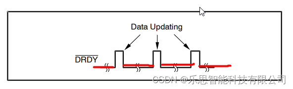
From the above picture, we can know that in the t17 stage, the data cannot be read. In addition, the minimum is 16 τCLKIN. The specific number is related to the DATA_rate setting you configured.
1.6 Synchronous SYNC timing
To synchronize SYNC, either use the SYNC pin or issue the SYNC command. What we plan to do here is to issue the SYNC command.
2. Discrete components
2.1 INPUT MULTIPLEXER input channel selector
At the same time, there can only be one channel input, so the selection control of the input channel is controlled by the MULTIPLEXER register. AINp is positive, if single-ended input is used
into, then AINN is grounded.
remind:
2.2 OPEN/SHORT SENSOR DETECTION Open/short sensor detection
The Sensor Detection Current Source (SDCS) provides a method to verify the integrity of external sensors connected to the ADS1255/6. (To be honest, I didn’t understand, it was embarrassing)
It doesn’t matter, we will turn off this sensor detection. My personal guess is that it may be used to determine whether a signal is input to the analog input terminal and whether it is an open circuit or a short circuit state.
When SDCS is enabled, ADS1256 will automatically open the buffer of the analog input terminal, regardless of the bit setting of the buffer. Doing this prevents input signals from loading signals from SDCS.
All in all, I don’t understand much about the simulation part, but what we can know is that if SDCS is turned on, it can prevent measurements when there is an open circuit or a short circuit.
2.3 PGA (programmable gain amplifier)
The meaning of the above table is very interesting. The settings of the PGA are not set casually. When a particularly small signal is to be measured, the PGA is very useful. In this regard, the appropriate PGA must be selected based on the maximum input voltage of the full scale. The PGA settings are in the ADCON register.
important:
After changing the settings of the PGA, the A/D converter needs to be recalibrated
2.4 DIGITAL FILTER (digital filter)
There can be a trade-off between data rate (sampling rate) and resolution.
The data rate configuration is set in DRATE.
The following is the amplitude frequency response
3 modes
First of all, let me talk about the concept of SETTLING TIME in the AD1256 chip.
The settling time refers to the propagation delay from the analog input to the digital filter. The SETTLING TIME corresponds differently to different data rates. Using different modes will produce different setting times.
It doesn’t matter if DRDY_n is used as an input signal, ADS1256 will send a low level to indicate that we can start reading data.
The following are all after the initialization settings based on buffer, PGA, and datarate are completed. Take the mode selection.
3.1 Single channel synchronization mode
After initialization is completed, after sending a synchronization command or a synchronization command through the SYNC/PWND pin, enter the setting time (t18).
Then issue the RDATA command when DRDY_n is at low level, and then read.
This mode is also very simple.
3.2 Use the input selector to switch channels
The most effective way to switch (cycle through) and change the input channel is to use the WREG command to the MUX register. After DRDY_n goes low, issue the WREG command, then change the channel, restart the conversion by issuing the SYNC and WAKEUP commands, and issue it with RDATA Read data after command. And here we have to pay attention. When the input channel switches, we do not need to discard the data at all, because ADS1256 can fully obtain stable data before DRDY_n goes low to indicate that the read data is ready. However, when reading data, it is the data of the previous channel that is read. When DRDY_n goes low again, the cycle repeats by updating the multi-channel register.
3.3 Use single-shot mode (energy-saving mode)
Using the STANDBY command can greatly reduce power consumption, and you can convert from standby mode to one-shot by issuing the wakeup command. Using this mode, there is an additional delay required for the ADC’s modulator to start up and stabilize.
3.4 Continuous conversion mode (RDATAC)
This mode means that the conversion only requires one RATAC, without sending an rdata and reading a DOUT.
This continuous conversion reading method can be used after synchronization, input register changes, or after waking up from standby mode. Everything else is the same in this method, except that reading no longer involves sending an rdata and then reading the data. Instead, you only need to send rdatac once, and then directly read the data at the low level of drdy_n. But this depends on the number of cycles of DRDY_n. The figure below shows the periods of DRDY_n corresponding to different SPS. If you do not read periodically, you may read a mixture of old data and new data.
Therefore, I do not recommend this continuous reading mode, and we will not implement it here. Even if it is implemented, I think it can only be achieved in the case of single-channel acquisition.
4. Calibration
OFC calibration: offset calibration
FSC calibration: full-scale calibration
DRDY_n goes high when calibration begins and remains so until settled data is ready afterwards.
DRDY_n will keep going high, when calibration begins, until the data is ready.
The following paragraph is very critical. Self-verification must be performed after reset, power-on, buffer change, data rate change, and PGA change.
The following are the ideal OFC and FSC under different data rates, but this is not important at all. We can just leave it to the system to automatically verify it, without specifically writing it through the register.
4.1 Self-calibration self-calibration
The above official recommendations strongly recommend using the SELFCAL command after powering on. Although automatic self-verification is configured.
Use the three commands SELFOCAL, SELFGCAL, and SELFCAL
/*
*************************************************** *************************************************** *****
*
*Module name: ADS125X driver module (8-channel 24-bit ADC with PGA)
* File name: bsp_ADS125X.h
*
* Copyright (C), 2013-2014, Armfly Electronics www.armfly.com
*
*************************************************** *************************************************** *****
*/

#ifndef _BSP_ADS125X_H
#define _BSP_ADS125X_H

#include "main.h"


#define ADC_DEBUG 0


//define commands
#define ADS1256_CMD_WAKEUP 0x00
#define ADS1256_CMD_RDATA 0x01
#define ADS1256_CMD_RDATAC 0x03
#define ADS1256_CMD_SDATAC 0x0f
#define ADS1256_CMD_RREG 0x10
#define ADS1256_CMD_WREG 0x50
#define ADS1256_CMD_SELFCAL 0xf0
#define ADS1256_CMD_SELFOCAL 0xf1
#define ADS1256_CMD_SELFGCAL 0xf2
#define ADS1256_CMD_SYSOCAL 0xf3
#define ADS1256_CMD_SYSGCAL 0xf4
#define ADS1256_CMD_SYNC 0xfc
#define ADS1256_CMD_STANDBY 0xfd
#define ADS1256_CMD_REST 0xfe

// define the ADS1256 register values
#define ADS1256_STATUS 0x00
#define ADS1256_MUX 0x01
#define ADS1256_ADCON 0x02
#define ADS1256_DRATE 0x03
#define ADS1256_IO 0x04
#define ADS1256_OFC0 0x05
#define ADS1256_OFC1 0x06
#define ADS1256_OFC2 0x07
#define ADS1256_FSC0 0x08
#define ADS1256_FSC1 0x09
#define ADS1256_FSC2 0x0A


// define multiplexer codes
#define ADS1256_MUXP_AIN0 0x00
#define ADS1256_MUXP_AIN1 0x10
#define ADS1256_MUXP_AIN2 0x20
#define ADS1256_MUXP_AIN3 0x30
#define ADS1256_MUXP_AIN4 0x40
#define ADS1256_MUXP_AIN5 0x50
#define ADS1256_MUXP_AIN6 0x60
#define ADS1256_MUXP_AIN7 0x70
#define ADS1256_MUXP_AINCOM 0x80

#define ADS1256_MUXN_AIN0 0x00
#define ADS1256_MUXN_AIN1 0x01
#define ADS1256_MUXN_AIN2 0x02
#define ADS1256_MUXN_AIN3 0x03
#define ADS1256_MUXN_AIN4 0x04
#define ADS1256_MUXN_AIN5 0x05
#define ADS1256_MUXN_AIN6 0x06
#define ADS1256_MUXN_AIN7 0x07
#define ADS1256_MUXN_AINCOM 0x08


//define gain codes
#define ADS1256_GAIN_1 0x00
#define ADS1256_GAIN_2 0x01
#define ADS1256_GAIN_4 0x02
#define ADS1256_GAIN_8 0x03
#define ADS1256_GAIN_16 0x04
#define ADS1256_GAIN_32 0x05
#define ADS1256_GAIN_64 0x06
//#define ADS1256_GAIN_64 0x07

//define drate codes
#define ADS1256_DRATE_30000SPS 0xF0
#define ADS1256_DRATE_15000SPS 0xE0
#define ADS1256_DRATE_7500SPS 0xD0
#define ADS1256_DRATE_3750SPS 0xC0
#define ADS1256_DRATE_2000SPS 0xB0
#define ADS1256_DRATE_1000SPS 0xA1
#define ADS1256_DRATE_500SPS 0x92
#define ADS1256_DRATE_100SPS 0x82
#define ADS1256_DRATE_60SPS 0x72
#define ADS1256_DRATE_50SPS 0x63
#define ADS1256_DRATE_30SPS 0x53
#define ADS1256_DRATE_25SPS 0x43
#define ADS1256_DRATE_15SPS 0x33
#define ADS1256_DRATE_10SPS 0x23
#define ADS1256_DRATE_5SPS 0x13
#define ADS1256_DRATE_2_5SPS 0x03

//void Init_ADS1256_GPIO(void);
//void Delay(unsigned int dal);
void ADS1256_Init(uint8_t PGA); //Initialize ADS1256

int32_t ADS1256ReadData(void);
int32_t ADS_sum(unsigned char road);
int32_t ADS_Diff(unsigned char channel);
#endif

/************************************ Armfly Electronics www.armfly.com (END OF FILE) ******* ******************************/
#include "bsp_ads125x.h"
#include "main.h"

/*
ADS125X basic features:
1. The analog part is powered by 5V;
2. SPI digital interface level: 3.3V
3. PGA setting range: 1, 2, 4, 8, 16, 32, 64,
4. Reference voltage 2.5V (recommended default, external)
5. Input voltage range: When PGA = 1, plus or minus 5V can be input
6. Automatic calibration (when PGA, BUF enable, and data sampling rate are set, self-calibration will be started)
7. The input buffer can be enabled and disabled (usually enabled)


External crystal frequency = 7.68MHz,
Clock frequency tCLK = 1/7.68M = 0.13uS
Output data period tDATA = 1 / 30K = 0.033mS (calculated based on 30Ksps)

Clock speed requirements for SPI: (ADS125X.pdf page 6)
Fastest 4 tCLK = 0.52uS
The slowest 10 tDATA = 0.3mS (calculated based on 30Ksps)

SCL high level and low level duration minimum 200ns

After the RREG, WREG, RDATA command, a delay of 4 * tCLK = 0.52uS is required;
After RDATAC, RESET, SYNC commands, a delay of 24 * tCLK = 3.12uS is required;

Actual test, after powering on 3.3V, without any configuration, the DRDY port line of ADS125 starts to output pulse signals (2.6us high, 33.4 low, frequency 30KHz)
*/

/*
debug log
(1) When setting the register, SCK is too fast and the chip cannot receive data every time. Reason: There is a small delay between sending adjacent bytes.
(2) When the CPU is continuously reset, the chip output sampling rate occasionally appears abnormal.
*/


/* Define macros for setting port lines to 0 and 1 */

#define RESET_0() HAL_GPIO_WritePin(SPI2_RST_GPIO_Port, SPI2_RST_Pin,GPIO_PIN_RESET);//GPIO_ResetBits(SPI2_RST_GPIO_Port, SPI2_RST_Pin)
#define RESET_1() HAL_GPIO_WritePin(SPI2_RST_GPIO_Port, SPI2_RST_Pin,GPIO_PIN_SET);

#define CS_0() HAL_GPIO_WritePin(SPI2_CS_GPIO_Port, SPI2_CS_Pin,GPIO_PIN_RESET);
#define CS_1() HAL_GPIO_WritePin(SPI2_CS_GPIO_Port, SPI2_CS_Pin,GPIO_PIN_SET);

#define SCK_0() HAL_GPIO_WritePin(SPI2_CLK_GPIO_Port, SPI2_CLK_Pin,GPIO_PIN_RESET);
#define SCK_1() HAL_GPIO_WritePin(SPI2_CLK_GPIO_Port, SPI2_CLK_Pin,GPIO_PIN_SET);

#define DI_0() HAL_GPIO_WritePin(SPI2_DIN_GPIO_Port, SPI2_DIN_Pin,GPIO_PIN_RESET);
#define DI_1() HAL_GPIO_WritePin(SPI2_DIN_GPIO_Port, SPI2_DIN_Pin,GPIO_PIN_SET);

#define DO_IS_HIGH() (HAL_GPIO_ReadPin(SPI2_DOUT_GPIO_Port, SPI2_DOUT_Pin) == GPIO_PIN_SET)

#define DRDY_IS_LOW() (HAL_GPIO_ReadPin(SPI2_NDY_GPIO_Port, SPI2_NDY_Pin ) == GPIO_PIN_RESET)


void ADS1255_SELFCAL(void);
void ADS1255_SELFOCAL(void);
void ADS1255_SELFGCAL(void);
void ADS1255_SYSOCAL(void);
void ADS1255_WAKEUP(void);
void ADS1255_RESET(void);
void ADS1255_SYNC(void);
void ADS1255_RDATAC(void);

uint8_t choice_flag=0;
/*
*************************************************** *************************************************** *****
* Function name: delay_us
* Function description: Configure the GPIO and SPI interface of STM32 for connecting to ADS125X
*Formal parameters: none
* Return value: None
*************************************************** *************************************************** *****
*/
void delay_us(uint32_t udelay)
{<!-- -->
uint32_t Delay = udelay * 120/4;
do
{<!-- -->
__NOP();
}
while (Delay --);
}

/*
*************************************************** *************************************************** *****
* Function name: bsp_InitADS125X
* Function description: Configure the GPIO and SPI interface of STM32 for connecting to ADS125X
*Formal parameters: none
* Return value: None
*************************************************** *************************************************** *****
*/
void bsp_InitADS125X(void)
{<!-- -->
    RESET_1();
    CS_1();
    SCK_0(); /* When the SPI bus is idle, the clock line is low */
    DI_1();
\t
    HAL_Delay(100);
    RESET_0();
    HAL_Delay(100);
    RESET_1();
    HAL_Delay(100);
    CS_1();
    HAL_Delay(1);
    SCK_0(); /* When the SPI bus is idle, the clock line is low */
    HAL_Delay(1);
    CS_0();
    HAL_Delay(1);
}

//Several delays
static void ADS125X_DelaySCLK(void)//F103 72M
{<!-- -->
    uint16_t i;
    for(i = 0; i < 5; i + + );//0.5us
}
void ADS125X_Delay_1us(uint16_t t)//F103 72M
{<!-- -->
    uint16_t i, j;

    for(j = 0; j < t; j + + )
    {<!-- -->
        for(i = 0; i < 10; i + + );//1us
    }
}
static void ADS1256_DelayDATA(void)
{<!-- -->
    /*
    Delay from last SCLK edge for DIN to first SCLK rising edge for DOUT: RDATA, RDATAC,RREG Commands
    Minimum 50 tCLK = 50 * 0.13uS = 6.5uS
    */
    ADS125X_Delay_1us(10); /* Minimum delay 6.5uS, take 10us here */

}


/*
*************************************************** *************************************************** *****
* Function name: ADS125X_Send8Bit
* Function description: Send 8 bits of data to the SPI bus. Without CS control.
*Formal parameter: _data: data
* Return value: None
*************************************************** *************************************************** *****
*/
static void ADS125X_Send8Bit(uint8_t _data)
{<!-- -->
    uint8_t i;

    /* When sending multiple bytes continuously, a delay is required */
    ADS125X_DelaySCLK();
    ADS125X_DelaySCLK();

    /* ADS125X requires SCL high level and low level duration to be at least 200ns */
    for(i = 0; i < 8; i + + )
    {<!-- -->
        if(_data & 0x80)
        {<!-- -->
            DI_1();
        }
        else
        {<!-- -->
            DI_0();
        }
        SCK_1();
        ADS125X_DelaySCLK();
        _data <<= 1;
        SCK_0(); /* <---- ADS125X samples DIN data on the falling edge of SCK, and the data must be maintained for 50nS */
        ADS125X_DelaySCLK();
    }
}

/*
*************************************************** *************************************************** *****
* Function name: ADS125X_Recive8Bit
* Function description: Receive 8 bits of data from the SPI bus. Without CS control.
*Formal parameters: none
* Return value: None
*************************************************** *************************************************** *****
*/
static uint8_t ADS125X_Recive8Bit(void)
{<!-- -->
    uint8_t i;
    uint8_t read = 0;

    ADS125X_DelaySCLK();
    /* ADS125X requires SCL high level and low level duration to be at least 200ns */
    for(i = 0; i < 8; i + + )
    {<!-- -->
        SCK_1();
        ADS125X_DelaySCLK();
        read = read << 1;
        SCK_0();
        if(DO_IS_HIGH())
        {<!-- -->
            read++;
        }
        ADS125X_DelaySCLK();
    }
    return read;
}
//ADS1256 write data
//Write a byte databyte to the register with address regaddr in ADS1256
void ADS1256WREG(unsigned char regaddr, unsigned char databyte)
{<!-- -->
    CS_0();
    //Write data address to register
    ADS125X_Send8Bit(ADS1256_CMD_WREG | (regaddr & amp; 0x0F));
    //Number of written data n-1
    ADS125X_Send8Bit(0x00);
    //Write data databyte to the register pointed to by regaddr address
    ADS125X_Send8Bit(databyte);
    CS_1();
}


//ADS1255 read register
//Description: Write the register address as required
unsigned char ADS1256RREG(unsigned char regaddr)
{<!-- -->
    unsigned char reg_date;
    CS_0();
    //Write data address to register
    ADS125X_Send8Bit(regaddr | ADS1256_CMD_RREG);
    //Number of written data n-1
    ADS125X_Send8Bit(0x00);
    reg_date = ADS125X_Recive8Bit();
    CS_1();
    return reg_date;
}

//ADS1255 write register
void ADS1256_WriteCmd(unsigned char _cmd)
{<!-- -->
    CS_0();
    ADS125X_Send8Bit(_cmd);
    CS_1();
}

//Set single-ended acquisition channel
void ADS1256_SetChannal(uint8_t _ch)
{<!-- -->
    /*
    Bits 7-4 PSEL3, PSEL2, PSEL1, PSEL0: Positive Input Channel (AINP) Select
    0000 = AIN0 (default)
    0001 = AIN1
    0010 = AIN2 (ADS1256 only)
    0011 = AIN3 (ADS1256 only)
    0100 = AIN4 (ADS1256 only)
    0101 = AIN5 (ADS1256 only)
    0110 = AIN6 (ADS1256 only)
    0111 = AIN7 (ADS1256 only)
    1xxx = AINCOM (when PSEL3 = 1, PSEL2, PSEL1, PSEL0 are ?°don?ˉt care?±)

    NOTE: When using an ADS1255 make sure to only select the available inputs.

    Bits 3-0 NSEL3, NSEL2, NSEL1, NSEL0: Negative Input Channel (AINN)Select
    0000 =AIN0
    0001 = AIN1 (default)
    0010 = AIN2 (ADS1256 only)
    0011 = AIN3 (ADS1256 only)
    0100 = AIN4 (ADS1256 only)
    0101 = AIN5 (ADS1256 only)
    0110 = AIN6 (ADS1256 only)
    0111 = AIN7 (ADS1256 only)
    1xxx = AINCOM (when NSEL3 = 1, NSEL2, NSEL1, NSEL0 are ?°don?ˉt care?±)
    */
    if(_ch > 2)
    {<!-- -->
        return;
    }
    ADS1256WREG(ADS1256_MUX, (_ch << 4) | (1 << 3)); /* Bit3 = 1, AINN 1ì?¨?ó AINCOM */
}

//Set the differential acquisition channel
void ADS1256_SetDiffChannal(uint8_t _ch)
{<!-- -->
    /*
    Bits 7-4 PSEL3, PSEL2, PSEL1, PSEL0: Positive Input Channel (AINP) Select
    0000 = AIN0 (default)
    0001 = AIN1
    0010 = AIN2 (ADS1256 only)
    0011 = AIN3 (ADS1256 only)
    0100 = AIN4 (ADS1256 only)
    0101 = AIN5 (ADS1256 only)
    0110 = AIN6 (ADS1256 only)
    0111 = AIN7 (ADS1256 only)
    1xxx = AINCOM (when PSEL3 = 1, PSEL2, PSEL1, PSEL0 are ?°don?ˉt care?±)

    NOTE: When using an ADS1255 make sure to only select the available inputs.

    Bits 3-0 NSEL3, NSEL2, NSEL1, NSEL0: Negative Input Channel (AINN)Select
    0000 =AIN0
    0001 = AIN1 (default)
    0010 = AIN2 (ADS1256 only)
    0011 = AIN3 (ADS1256 only)
    0100 = AIN4 (ADS1256 only)
    0101 = AIN5 (ADS1256 only)
    0110 = AIN6 (ADS1256 only)
    0111 = AIN7 (ADS1256 only)
    1xxx = AINCOM (when NSEL3 = 1, NSEL2, NSEL1, NSEL0 are ?°don?ˉt care?±)
    */
    if(_ch == 0)
    {<!-- -->
        ADS1256WREG(ADS1256_MUX, (0 << 4) | 1); /* Differential input AIN0, AIN1 */
    }
    else if(_ch == 1)
    {<!-- -->
        ADS1256WREG(ADS1256_MUX, (2 << 4) | 3); /* Differential input AIN2, AIN3 */
    }
    else if(_ch == 2)
    {<!-- -->
        ADS1256WREG(ADS1256_MUX, (4 << 4) | 5); /* Differential input AIN4, AIN5 */
    }
    else if(_ch == 3)
    {<!-- -->
        ADS1256WREG(ADS1256_MUX, (6 << 4) | 7); /* Differential input AIN6, AIN7 */
    }
}

//wait
void ADS1256_WaitDRDY(void)
{<!-- -->
    uint32_t i;

    for(i = 0; i < 40000000; i + + )
    {<!-- -->
        if(DRDY_IS_LOW())
        {<!-- -->
            break;
        }
    }
    if(i >= 40000000)
    {<!-- -->
#if ADC_DEBUG
        printf("ADS1256_WaitDRDY() Time Out ...\r\
"); /* Debugging statements. Terms for troubleshooting */
#endif
    }
}

//Initialize ADS1256
void ADS1256_Init(uint8_t PGA)
{<!-- -->
    /* initialization */
    bsp_InitADS125X();
    HAL_Delay(10);
    /* configuration */
    ADS1256_WriteCmd(ADS1256_CMD_REST);
    HAL_Delay(100);
    ADS1256_WriteCmd(ADS1256_CMD_SYNC);
    HAL_Delay(10);
    ADS1256_WriteCmd(ADS1256_CMD_WAKEUP);
    HAL_Delay(10);
    /* AD configuration */
// ADS1256WREG(ADS1256_STATUS, 0x04); // High bit first, self-calibration, no buffering
    ADS1256WREG(ADS1256_STATUS, 0x06); // High bit first, self-calibration, use buffer to measure lower than 3.5V
    HAL_Delay(10);
    ADS1256WREG(ADS1256_MUX, 0x08); //Initialize port A0 to +’, AINCOM bit -’
// ADS1256WREG(ADS1256_MUX, 0x01); // Initialize port A0 to +’, A1 bit -’ differential
    HAL_Delay(10);
    ADS1256WREG(ADS1256_ADCON, 0x00); //
    ADS1256WREG(ADS1256_ADCON, PGA); // PGA sets the gain multiple. Turn off the CLKOUT pin output, turn off sensor detection, and set the gain multiple to 1.
HAL_Delay(10);
    ADS1256WREG(ADS1256_DRATE, ADS1256_DRATE_50SPS); // Data 50sps
    HAL_Delay(10);
    ADS1256WREG(ADS1256_IO, 0x00);
    HAL_Delay(10);

    /* Calibration */
    ADS125X_Send8Bit(0xF0);
    HAL_Delay(100);
choice_flag=PGA;
}

//Read AD value
int32_t ADS1256ReadData(void)
{<!-- -->
    uint32_t read = 0;
    /* SPI chip select = 0 */
    CS_0();

    /* Command to read data */
    ADS125X_Send8Bit(ADS1256_CMD_RDATA);

    /* Must be delayed before reading the chip return data */
    ADS1256_DelayDATA();

    /* Read the sampling result, 3 bytes, high byte first */
    read = ADS125X_Recive8Bit() << 16;
    read + = (ADS125X_Recive8Bit() << 8);
    read + = ADS125X_Recive8Bit();
\t
    /* SPI chip select = 1 */
    CS_1();

    /* Expand negative numbers. 24-bit signed number is expanded to 32-bit signed number */
    if(read & 0x800000)
    {<!-- -->
        read + = 0xFF000000;
    }

    return (int32_t)read;
}


uint8_t ADS1255_ReadID(void)
{<!-- -->
// uint8_t id=0;
// uint8_t buff;
// /*SPI=0*/
// CS_0();
// /* Configuration */
// ADS1256_WriteCmd(ADS1256_CMD_RREG);
// HAL_Delay(100);
// ADS1256_WriteCmd(ADS1256_CMD_SYNC);
// HAL_Delay(10);
// ADS1256_WriteCmd(ADS1256_CMD_WAKEUP);
// HAL_Delay(10);
//
//
\t
// buff=CMD_RREG|REG_STATUS;
// HAL_SPI_Transmit( & amp;hspi2, & amp;buff,1,SPIx_TIMEoUT_MAX); //SPI
// buff=0x00;
// HAL_SPI_Transmit( & amp;hspi2, & amp;buff,1,SPIx_TIMEoUT_MAX); //SPI
// while(HAL_GPIO_ReadPin(DRDY_GPIO_Port,DRDY_Pin));
// HAL_Delay(1);
// HAL_SPI_Receive( & amp;hspi2, & amp;id,1,SPIx_TIMEoUT_MAX);
// /*SPI=1*/
// HAL_GPIO_WritePin(SPI2_NSS_GPIO_Port,SPI2_NSS_Pin,GPIO_PIN_SET);
// return (id>>4);
return 0;
}


//Read ADS1256 single channel data
int32_t ADS_sum(unsigned char channel)
{<!-- -->
    /* wait */
// ADS1256_WaitDRDY();
    /* Switch analog channel */
    ADS1256_SetChannal(channel);//Single-ended
//ADS1256_SetDiffChannal(0);//Difference
    ADS125X_Delay_1us(5);
    /* Synchronize */
    ADS1256_WriteCmd(ADS1256_CMD_SYNC);
    ADS125X_Delay_1us(5);
    /* Wake up */
    ADS1256_WriteCmd(ADS1256_CMD_WAKEUP);
    ADS125X_Delay_1us(25);
    /* Read the AD value and return 24-bit data */
    return (int32_t)ADS1256ReadData();
}
//Read ADS1256 differential data
int32_t ADS_Diff(unsigned char channel)
{<!-- -->
    /* wait */
// ADS1256_WaitDRDY();
    /* Switch analog channel */
//ADS1256_SetChannal(channel);//Single-ended
    ADS1256_SetDiffChannal(0);//Difference
// ADS125X_Delay_1us(5);
    /* Synchronize */
    ADS1256_WriteCmd(ADS1256_CMD_SYNC);
// ADS125X_Delay_1us(5);
    /* Wake up */
    ADS1256_WriteCmd(ADS1256_CMD_WAKEUP);
// ADS125X_Delay_1us(25);
    /* Read the AD value and return 24-bit data */
    return (int32_t)ADS1256ReadData();
}
1. During the test, it was found that the data read by the communication was sometimes large and sometimes small. Finally, it was found that the document was a problem with the signal polarity and edge number set by the SPI. After the number was changed to 2, the test communication was stable and normal.

The default edge setting is 1, but it is actually more stable to use 2.

After changing to 2, the communication is very stable


When DRDY goes low, the AD value can be read.

CS enable must be low to read data from the ADC.


Shandong Boos
https://www.bos-power.com/product/751.html