This article only provides corresponding program instructions and simple chip instructions on how to use STM32 to control and cascade dot matrix screens using MAX7219. For specific chip instructions, please find the data manual (it is easiest to find a Taobao merchant)< /strong>
Table of Contents
1. Brief introduction to the chip
1. Chip pin configuration
1.1 Pin description
2. Timing diagram
2.1 Data format
2. How to use
1. Single-byte writing function
2. Chip initialization
3. Display function
3. Cascade description
1. Brief introduction to the chip
1. Chip pin configuration

1.1 Pin Description
| tube Foot | Name | Function |
| 1 | DIN | Serial data input port. Data is loaded internally on the rising edge of the clock 16-bit register. |
| 2,3,5-8,10,11 | DIG 0–DIG 7 |
The eight data drive lines set the common cathode of the display to low level. when closed 7219 This pin outputs high level, 7221 presents high impedance. |
| 4,9 | GND | Ground wire (pin 4 and pin 9 must be grounded at the same time) |
| 12 | LOAD (MAX7219) |
Load data. When the last 16 bits of continuous data are on the rising edge of LOAD Locked. |
| CS (MAX7221) |
Chip select terminal. When this terminal is low, serial data is loaded into the shift register. device. The last 16 bits of continuous data are locked at the rising edge of the cs terminal. |
|
| 13 | CLK | Clock sequence input terminal. Maximum rate is 10MHz. On rising clock edge, the data is moved into the internal shift register. falling edge, data from DOUT terminal output. For MAX7221, only when the cs terminal is low level The clock input is valid only. |
| 14-17,20-23 | SEG A–SEG G, DP |
7-segment and decimal point driver, providing current to the display. When a segment driver When the device is turned off, this end of 7219 is at low level and 7221 is at high impedance. |
| 18 | SET | Connect to VDD through a resistor to increase segment current. |
| 19 | V + | Positive voltage input, + 5V |
| 24 | DOUT | Serial data output port, input data from DIN at 16.5 Valid at this end after clock cycles. When using multiple MAX7219/MAX7221 Use this end to facilitate expansion. |
2. Timing diagram

Through three-wire control, data transmission starts when CS is pulled low, and the high and low of the DIN pin when CLK changes from low to high represents 1 and 0. When CS changes from 0 to 1, the data will be stored inside the chip.
2.1 Data Format

The data format is shown in the figure above. One frame of data consists of 2 parts. The upper 8 bits are the address and the lower 8 bits are the data. The addresses range from 0 to 15, corresponding to the data register and control register respectively, as shown in the figure below:

Please refer to the official data manual for specific content. Here is only a brief description of the internals of the chip. It is mainly necessary to know how to use it.
2. How to use


I am using a common cathode dot matrix screen. From the register diagram, we can see that Digit0~7 actually controls rows 1~8 of the dot matrix screen. When the Digit command is given, it is equivalent to pulling the level low, so this row is Is low level, as long as the column is high, the light will be on, so write a program based on this feature.
1. Single-byte writing function
The first step in programming is to write a write function program through the timing diagram as follows.
/*The control macro of 3 pins determines the low-bit band operation*/
#define MAX7219_DIN PBout(5)
#define MAX7219_CS PBout(6)
#define MAX7219_CLK PBout(7)
void MAX7219_Write_byte(uint8_t data)//Single byte write
{
uint8_t i=0;
MAX7219_CS=0;//In order to prevent CS from not being pulled low, it is pulled low every time
for(i=8;i>0;i--)
{
MAX7219_CLK=0;
if(data & amp;0x80)//high bit first
{
MAX7219_DIN=1;
}
else
{
MAX7219_DIN=0;
}
data=data<<1;//Shift the highest bit to the left to change the second highest bit to the highest bit
MAX7219_CLK=1;
}
}
After the basic single-byte function is completed, for the convenience of use, we use the single-byte write function to write a write command function, as follows:
void MAX7219_Write_Command(uint8_t addr,uint8_t data)//Write command
{
MAX7219_Write_byte(addr);//Register address
MAX7219_Write_byte(data); //Data to be written
}
2. Chip initialization
First, initialize several control registers of the chip. The program is as follows:
/************Macro definition is convenient for modification and observation************************/
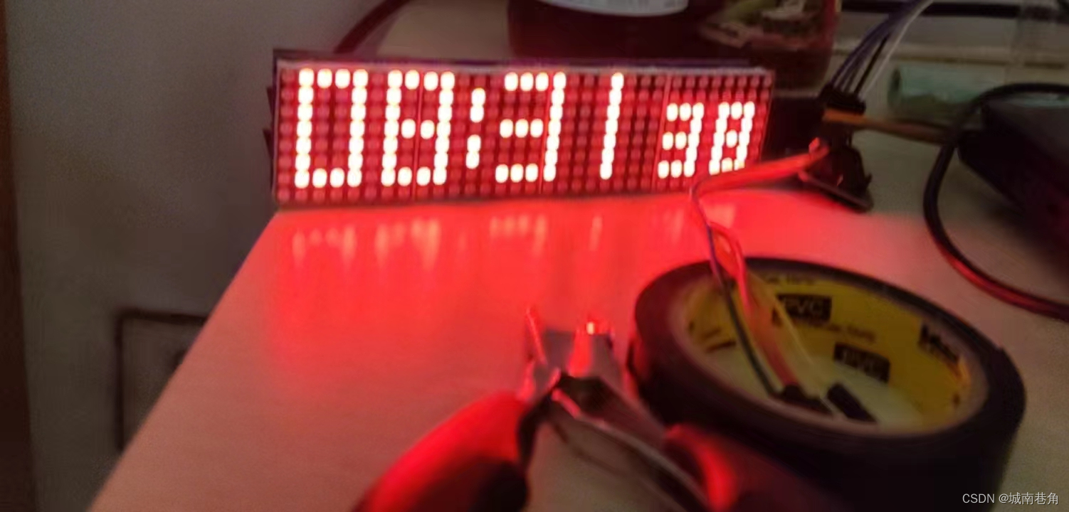
#define LEDCOUNT 4///The number of dot matrix screens I use 4 screens
#define DECODEMODE 0X09 //Encoding mode
#define INTENSITY 0X0A //Brightness
#define SCANLIMT 0x0B //Number of scan registers
#define SHUTDOWN 0X0C //Close register
#define DISPLAYTEST 0X0F //Display test
/****************************************************** /
void MAX7219_INIT(void)
{
uint8_t i=0;
GPIO_Config();
MAX7219_CS=0;
for(i=0;i<LEDCOUNT;i + + )
{
MAX7219_Write_Command(DECODEMODE,0X00);
/*Decoding register: 1 uses BCD code, 0 does not use (it is recommended to use BCD code for digital tube)*/
}
MAX7219_CS=1;//After sending 4 times here, CS is pulled high, then all 4 dot matrix screens receive the data and then load it into the register.
MAX7219_CS=0;
for(i=0;i<LEDCOUNT;i + + )
{
MAX7219_Write_Command(INTENSITY,0X01);
/*Brightness control: 0x00~0x0F 0 is the darkest, 0xFs is the brightest*/
}
MAX7219_CS=1;
MAX7219_CS=0;
for(i=0;i<LEDCOUNT;i + + )
{
MAX7219_Write_Command(SCANLIMT,0X07);
/*The number of lines of the dot matrix screen and the segment of the digital tube: 0 is 1 line, 7 is 8 lines*/
}
MAX7219_CS=1;
MAX7219_CS=0;
for(i=0;i<LEDCOUNT;i + + )
{
MAX7219_Write_Command(SHUTDOWN,0X01);
/*Power-down mode: 0 power-down mode 1 normal mode*/
}
MAX7219_CS=1;
MAX7219_CS=0;
for(i=0;i<LEDCOUNT;i + + )
{
MAX7219_Write_Command(DISPLAYTEST,0X00);
/*Display register: 0 normal mode 1 test mode*/
}
MAX7219_CS=1;
\t
}
3.Display function
After the initialization is completed, it can be displayed. The display function is as follows:
/*Font library defined by font library */
 const u8 _4x7Num[10][8]={
{0x0f,0x09,0x09,0x09,0x09,0x09,0x0f,0x00},//0
{0x02,0x02,0x02,0x02,0x02,0x02,0x02,0x00},//1
{0x0f,0x01,0x01,0x0f,0x08,0x08,0x0f,0x00},//2
{0x0f,0x01,0x01,0x0f,0x01,0x01,0x0f,0x00},//3
{0x09,0x09,0x09,0x0f,0x01,0x01,0x01,0x00},//4
{0x0f,0x08,0x08,0x0f,0x01,0x01,0x0f,0x00},//5
{0x0f,0x08,0x08,0x0f,0x09,0x09,0x0f,0x00},//6
{0x0f,0x01,0x01,0x01,0x01,0x01,0x01,0x00},//7
{0x0f,0x09,0x09,0x0f,0x09,0x09,0x0f,0x00},//8
{0x0f,0x09,0x09,0x0f,0x01,0x01,0x0f,0x00}//9
 };
for(i=1;i<9;i + + )//Line 1 to Line 8 of the dot matrix screen
{
MAX7219_CS=0;
for(j=0; j< 4; j + + )//Because there are 4 dot matrix screens, the same line needs to be sent 4 times
{
switch(j)//use switch just for convenience of viewing
{
case 0:
MAX7219_Write_byte(i);
MAX7219_Write_byte(_4x7Num[5][i-1]);
               //Control the high and low levels of the column. The row is low level, so the light turns on when the column is 1. If the data is
               //0xF0 Then this line is 4 on and 4 off.
break;
case 1:
MAX7219_Write_byte(i);
MAX7219_Write_byte(_4x7Num[6][i-1]);
break;
case 2:
MAX7219_Write_byte(i);
MAX7219_Write_byte(_4x7Num[7][i-1]);
break;
case 3:
MAX7219_Write_byte(i);
MAX7219_Write_byte(_4x7Num[8][i-1]);
break;
}
}
   MAX7219_CS=1;
}
3. Cascading instructions
A characteristic of the MAX7219 chip is that the data will be saved to the register only after CS generates a rising edge. When more than 16 bits are exceeded, when another bit is transmitted, it will overflow from OUT and be transferred to the next dot matrix screen. In the IN of max7219, the following table is a schematic diagram. The first time data is sent, the data is in MAX7219① at this time, as shown in ① in the table. At this time, CS does not pull high and continues to send data. When a bit is sent, such as 0, this The data at that time is as shown in ② in the table, then the highest bit sent for the first time will overflow into max7219 ②, and so on. When another bit is sent, such as 1, then it is as shown in ③ in the table. That is, when the first 16-bit data is sent in the method, the data will be in the first MAX7219. If CS is pulled high, the register will save the data. If it is not pulled high, when 2 bytes of data are sent again, the first 2 bytes of data will be pushed into the second MAX7219, and so on.
| MAX7219① | MAX7219② | ||||||||||||||||||||||||||||||||
| bit0 | 1 | 2~13 | 14 | bit15 | bit0 | 1 | 2~13 | 14 | bit15 | ||||||||||||||||||||||||
| ① | 1 | 0 | 1 | 0 | 1 | 1 | 0 | 1 | 0 | 1 | 1 | 1 | 0 | 1 | 0 | 1 | |||||||||||||||||
| ② | 0 | 1 | 0 | 1 | 0 | 1 | 1 | 0 | 1 | 0 | 1 | 1 | 1 | 0 | 1 | 0 | 1 | ||||||||||||||||
| ③ | 1 | 0 | 1 | 0 | 1 | 0 | 1 | 1 | 0 | 1 | 0 | 1 | 1 | 1 | 0 | 1 | 0 | 1 | |||||||||||||||
The knowledge points of the article match the official knowledge files, and you can further learn related knowledge. C Skill Tree Home Page Overview 193883 people are learning the system